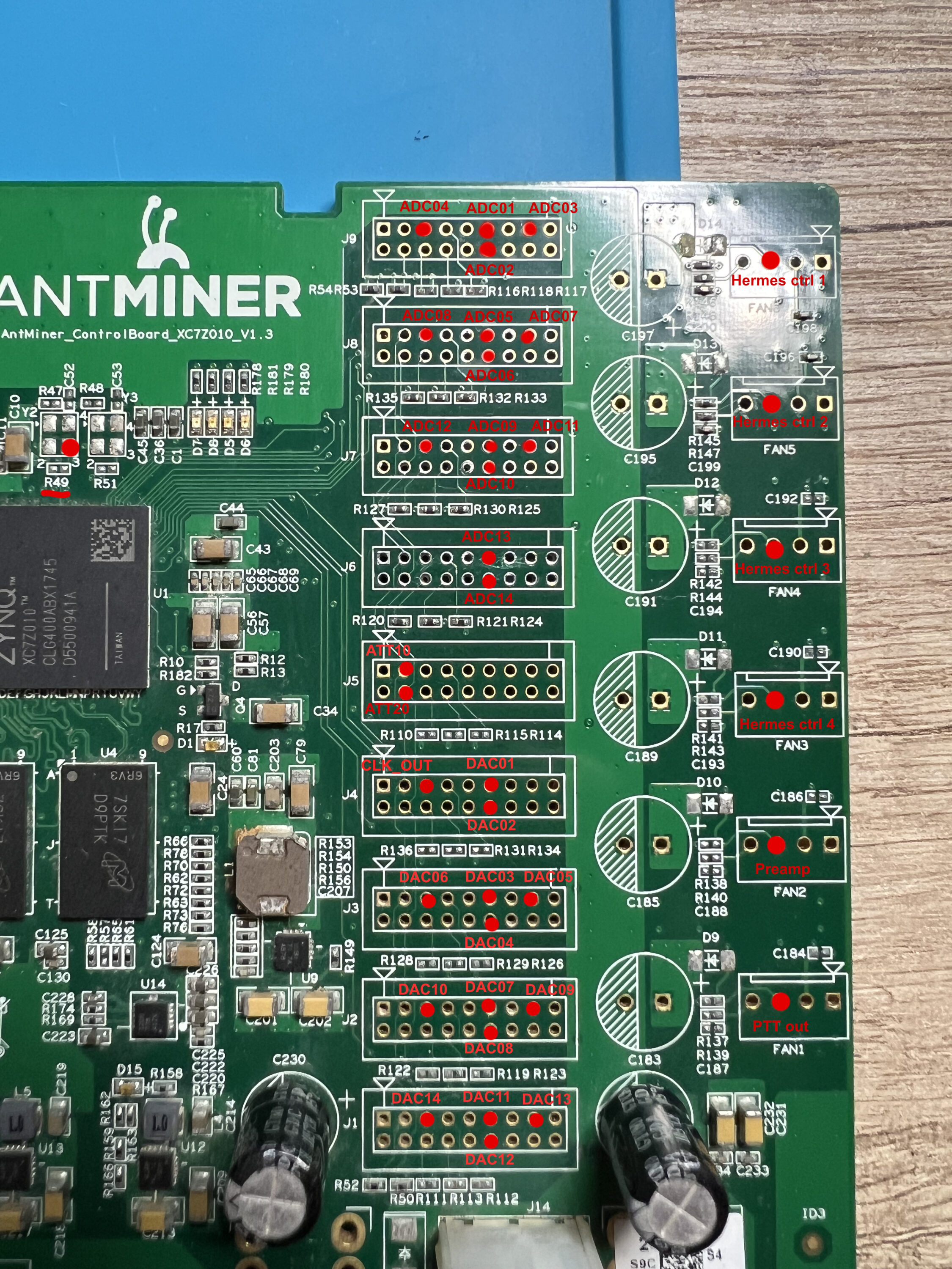
Pinout (ADC13-14 currently not in use, but reserved them and 2 more pins for 16bit ADC). Mind that on the photo ADC/DAC pins count from 1, on the actual DAC/ADC boards from 0, so on the DAC board 13 pin equals 14 pin on the antimner board.
ATTENTION — WIRE ORDER FOR DAC CHANGED, NOW IT STARTS IN REVERSIVE ORDER (12 == 0, 11 == 1 etcetera) (PHOTO WITH THE PREVIOUS ORDER)
Scheme:
I’m using 61.44 clock, it should be soldered to Y2 pad (red dot without caption on the photo), but do not forget to add resistor and capacitor like in scheme attached. I just soldered clock output to the R49 pad 🙂
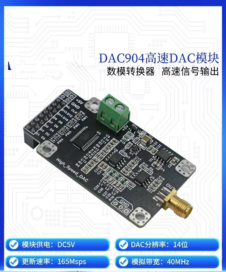
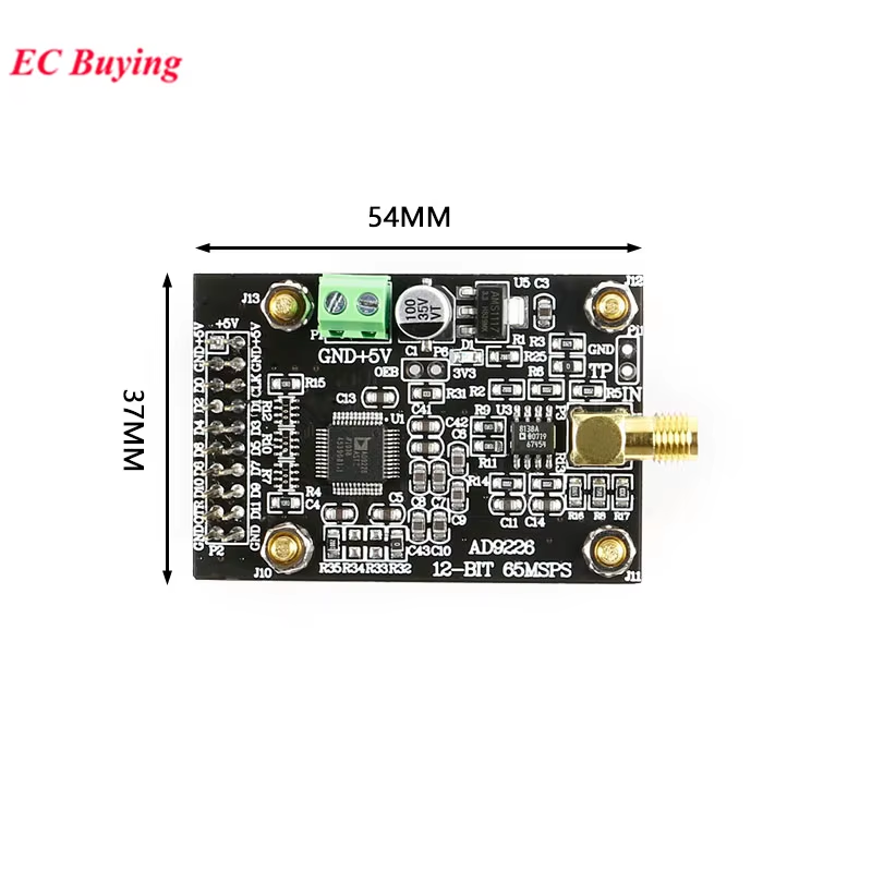
DAC:
https://aliexpress.ru/item/1005007209077013.html
ADC:
https://aliexpress.ru/item/1005003038271519.html?sku_id=12000045726984992
Clock — just typical single ended 61.44MHz 3.3v generator:
I bought this one — https://aliexpress.ru/item/10000282673529.html?spm=a2g2w.orderdetail.0.0.78e44aa6Vjj8Xh&sku_id=12000035895248861
It’s not so good, I bought it only for tests and posted here as an example.
All modules connected to the same clock generator — better to use coax cable.
You may want to find something better.
To boot from SD card set boot selection jumpers like that (first page on the scheme):
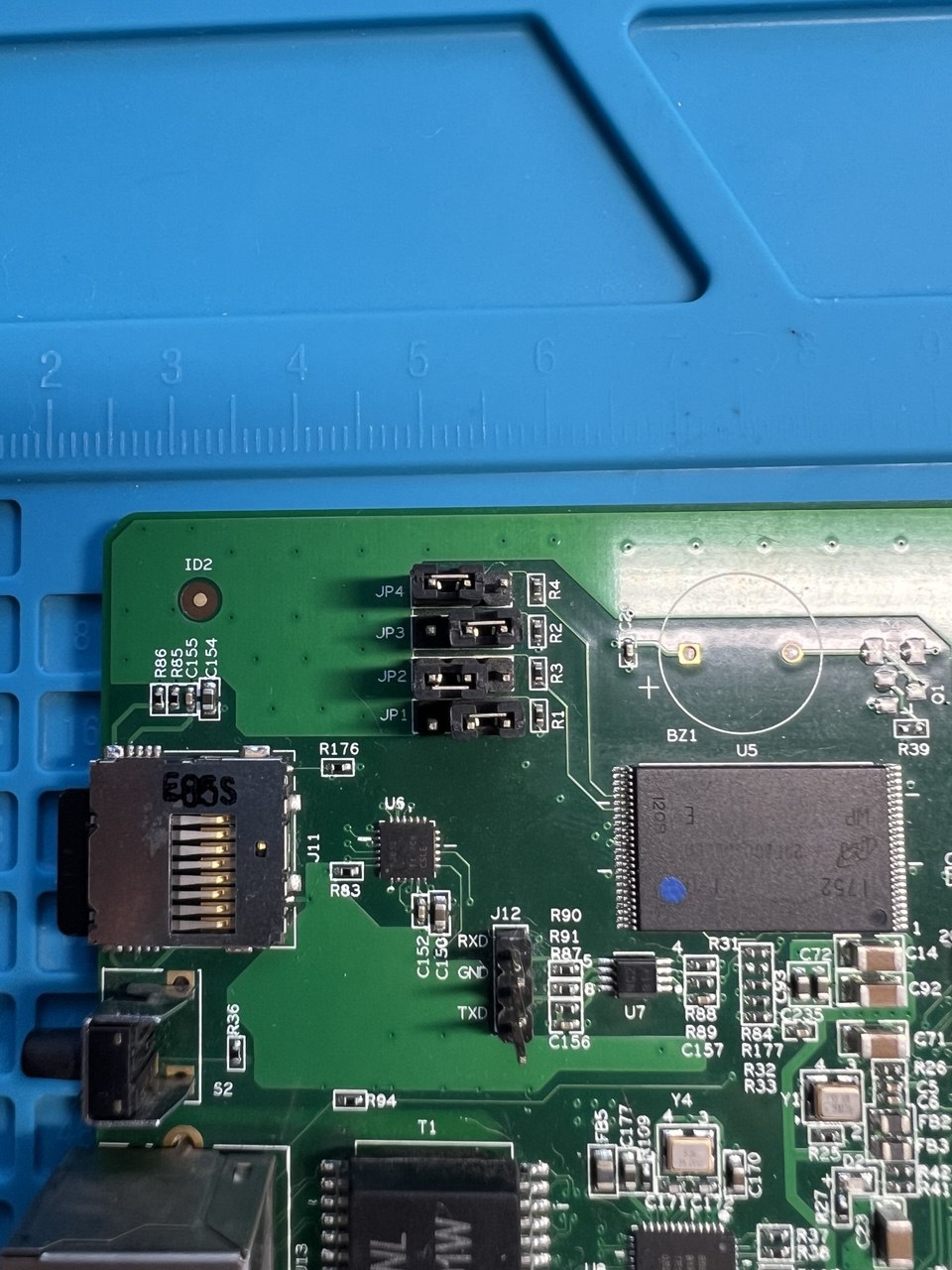
J12 — console UART input/output.
Power connector — 12v input with connector like for PC videocards:
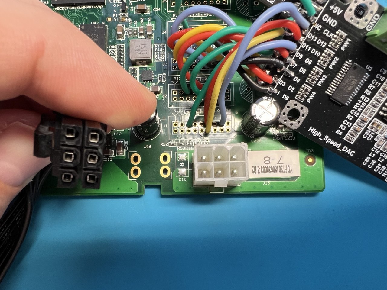
Top pins +12v, bottom — ground.
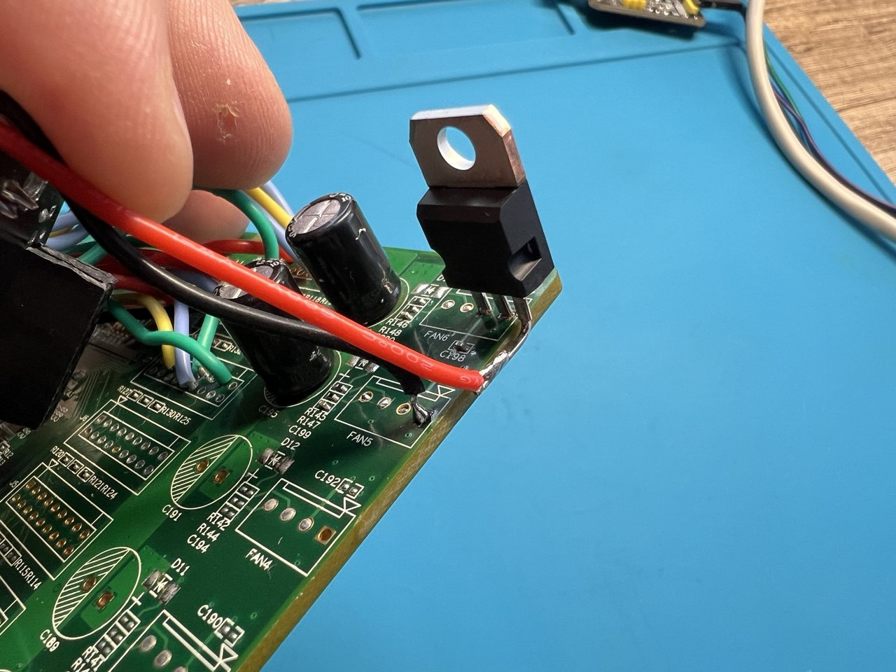
Board has +5v output, but you may want to use linear regulator, I soldered it to the fan pads:
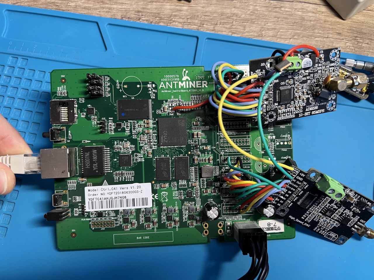
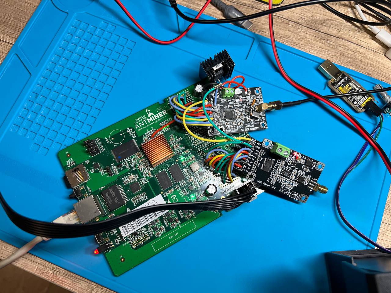
Full view: